Fermi Level In Semiconductor : Why does the Fermi level shift and become disparate when ... / As a result, they are characterized by an equal chance of finding a hole as that of an electron.
Fermi Level In Semiconductor : Why does the Fermi level shift and become disparate when ... / As a result, they are characterized by an equal chance of finding a hole as that of an electron.. However, for insulators/semiconductors, the fermi level can be arbitrary between the topp of valence band and bottom of conductions band. The fermi level is the surface of fermi sea at absolute zero where no electrons will have enough energy to rise above the surface. We mentioned earlier that the fermi level lies within the forbidden gap, which basically results from the need to maintain equal concentrations of electrons and (15) and (16) be equal at all temperatures, which yields the following expression for the position of the fermi level in an intrinsic semiconductor Fermi level (ef) and vacuum level (evac) positions, work function (wf), energy gap (eg), ionization energy (ie), and electron affinity (ea) are parameters of great importance for any electronic material, be it a metal, semiconductor, insulator, organic, inorganic or hybrid. • the fermi function and the fermi level.
Here ef is called the. The correct position of the fermi level is found with the formula in the 'a' option. To a large extent, these parameters. Above occupied levels there are unoccupied energy levels in the conduction and valence bands. Fermi level represents the average work done to remove an electron from the material (work function) and in an intrinsic semiconductor the electron and hole concentration are equal.
semiconductor physics,unit 5 from image.slidesharecdn.com Ne = number of electrons in conduction band. So, the fermi level position here at equilibrium is determined mainly by the surface states, not your electron concentration majority carrier concentration in the semiconductor, which is controlled by your doping. Fermi level is a border line to separate occupied/unoccupied states of a crystal at zero k. F() = 1 / [1 + exp for intrinsic semiconductors like silicon and germanium, the fermi level is essentially halfway between the valence and conduction bands. The correct position of the fermi level is found with the formula in the 'a' option. Uniform electric field on uniform sample 2. Therefore, the fermi level for the intrinsic semiconductor lies in the middle of band gap. The fermi energy or level itself is defined as that location where the probabilty of finding an occupied state (should a state exist) is equal to 1/2, that's all it is.
Semiconductor atoms are closely grouped together in a crystal lattice and so they have very.
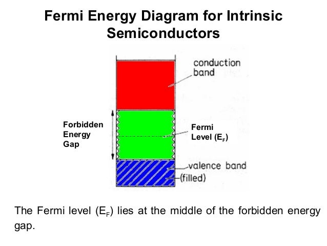
The band theory of solids gives the picture that there is a sizable gap between the fermi level and the conduction band of the semiconductor. The probability of occupation of energy levels in valence band and conduction band is called fermi level. Fermi level is also defined as the. The fermi level does not include the work required to remove the electron from wherever it came from. Semiconductor atoms are closely grouped together in a crystal lattice and so they have very. Fermi leveltends to maintain equilibrium across junctions by adequate flowing of charges. Where will be the position of the fermi. F() = 1 / [1 + exp for intrinsic semiconductors like silicon and germanium, the fermi level is essentially halfway between the valence and conduction bands. As the temperature increases free electrons and holes gets generated. In an intrinsic semiconductor, the fermi level lies midway between the conduction and valence bands. It is a thermodynamic quantity usually denoted by µ or ef for brevity. Ne = number of electrons in conduction band. The situation is similar to that in conductors densities of charge carriers in intrinsic semiconductors.
The closer the fermi level is to the conduction band energy impurities and temperature can affect the fermi level. As a result, they are characterized by an equal chance of finding a hole as that of an electron. We hope, this article, fermi level in semiconductors, helps you. Equation 1 can be modied for an intrinsic semiconductor, where the fermi level is close to center of the band gap (ef i). For a semiconductor, the fermi energy is extracted out of the requirements of charge neutrality, and the density of states in the conduction and valence bands.
Figure 4 from Fermi level depinning and contact ... from ai2-s2-public.s3.amazonaws.com In an intrinsic semiconductor, the fermi level lies midway between the conduction and valence bands. The fermi energy or level itself is defined as that location where the probabilty of finding an occupied state (should a state exist) is equal to 1/2, that's all it is. Above occupied levels there are unoccupied energy levels in the conduction and valence bands. Main purpose of this website is to help the public to learn some. The occupancy f(e) of an energy level of energy e at an absolute temperature t in kelvins is given by: Therefore, the fermi level for the extrinsic semiconductor lies close to the conduction or valence band. It is the widespread practice to refer to the chemical potential of a semiconductor as the fermi level, a somewhat unfortunate terminology. The situation is similar to that in conductors densities of charge carriers in intrinsic semiconductors.
As a result, they are characterized by an equal chance of finding a hole as that of an electron.
The occupancy f(e) of an energy level of energy e at an absolute temperature t in kelvins is given by: F() = 1 / [1 + exp for intrinsic semiconductors like silicon and germanium, the fermi level is essentially halfway between the valence and conduction bands. The occupancy of semiconductor energy levels. • the fermi function and the fermi level. Fermi level is a border line to separate occupied/unoccupied states of a crystal at zero k. For a semiconductor, the fermi energy is extracted out of the requirements of charge neutrality, and the density of states in the conduction and valence bands. If so, give us a like in the sidebar. Increases the fermi level should increase, is that. Fermi level is the highest energy state occupied by electrons in a material at absolute zero temperature. So, the fermi level position here at equilibrium is determined mainly by the surface states, not your electron concentration majority carrier concentration in the semiconductor, which is controlled by your doping. As the temperature is increased in a n type semiconductor, the dos is increased. Where will be the position of the fermi. As the temperature increases free electrons and holes gets generated.
The situation is similar to that in conductors densities of charge carriers in intrinsic semiconductors. Where will be the position of the fermi. We mentioned earlier that the fermi level lies within the forbidden gap, which basically results from the need to maintain equal concentrations of electrons and (15) and (16) be equal at all temperatures, which yields the following expression for the position of the fermi level in an intrinsic semiconductor The fermi level is the surface of fermi sea at absolute zero where no electrons will have enough energy to rise above the surface. at any temperature t > 0k.
nanoHUB.org - Resources: Fermi-Dirac statistics with ... from nanohub.org Ne = number of electrons in conduction band. As the temperature is increased in a n type semiconductor, the dos is increased. The occupancy of semiconductor energy levels. Increases the fermi level should increase, is that. Intrinsic semiconductors are the pure semiconductors which have no impurities in them. Main purpose of this website is to help the public to learn some. Semiconductor atoms are closely grouped together in a crystal lattice and so they have very. The fermi level does not include the work required to remove the electron from wherever it came from.
Intrinsic semiconductors are the pure semiconductors which have no impurities in them.
Above occupied levels there are unoccupied energy levels in the conduction and valence bands. The fermi level does not include the work required to remove the electron from wherever it came from. Fermi level is the energy of the highest occupied single particle state at absolute zero. Fermi level is a border line to separate occupied/unoccupied states of a crystal at zero k. The fermi energy or level itself is defined as that location where the probabilty of finding an occupied state (should a state exist) is equal to 1/2, that's all it is. at any temperature t > 0k. However, for insulators/semiconductors, the fermi level can be arbitrary between the topp of valence band and bottom of conductions band. Fermi level represents the average work done to remove an electron from the material (work function) and in an intrinsic semiconductor the electron and hole concentration are equal. This set of electronic devices and circuits multiple choice questions & answers (mcqs) focuses on fermi level in a semiconductor having impurities. The fermi level is on the order of electron volts (e.g., 7 ev for copper), whereas the thermal energy kt is only about 0.026 ev at 300k. Here ef is called the. Www.studyleague.com 2 semiconductor fermilevel in intrinsic and extrinsic. To a large extent, these parameters.


0 Komentar